- 您现在的位置:买卖IC网 > Sheet目录3882 > PIC16F74T-I/ML (Microchip Technology)IC MCU FLASH 4KX14 A/D 44QFN
2002 Microchip Technology Inc.
DS30325B-page 9
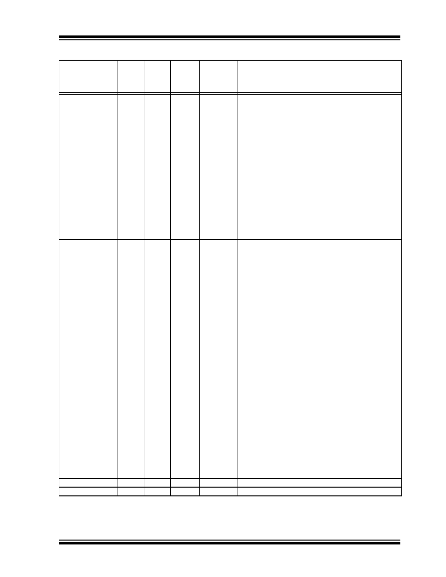
PIC16F7X
PORTB is a bi-directional I/O port. PORTB can be software
programmed for internal weak pull-up on all inputs.
RB0/INT
RB0
INT
21
18
I/O
I
TTL/ST(1)
Digital I/O.
External interrupt.
RB1
22
19
I/O
TTL
Digital I/O.
RB2
23
20
I/O
TTL
Digital I/O.
RB3/PGM
RB3
PGM
24
21
I/O
TTL
Digital I/O.
Low voltage ICSP programming enable pin.
RB4
25
22
I/O
TTL
Digital I/O.
RB5
26
23
I/O
TTL
Digital I/O.
RB6/PGC
RB6
PGC
27
24
I/O
TTL/ST(2)
Digital I/O.
In-Circuit Debugger and ICSP programming clock.
RB7/PGD
RB7
PGD
28
25
I/O
TTL/ST(2)
Digital I/O.
In-Circuit Debugger and ICSP programming data.
PORTC is a bi-directional I/O port.
RC0/T1OSO/T1CKI
RC0
T1OSO
T1CKI
11
8
I/O
O
I
ST
Digital I/O.
Timer1 oscillator output.
Timer1 external clock input.
RC1/T1OSI/CCP2
RC1
T1OSI
CCP2
12
9
I/O
I
I/O
ST
Digital I/O.
Timer1 oscillator input.
Capture2 input, Compare2 output, PWM2 output.
RC2/CCP1
RC2
CCP1
13
10
I/O
ST
Digital I/O.
Capture1 input/Compare1 output/PWM1 output.
RC3/SCK/SCL
RC3
SCK
SCL
14
11
I/O
ST
Digital I/O.
Synchronous serial clock input/output for SPI mode.
Synchronous serial clock input/output for I2C mode.
RC4/SDI/SDA
RC4
SDI
SDA
15
12
I/O
I
I/O
ST
Digital I/O.
SPI data in.
I2C data I/O.
RC5/SDO
RC5
SDO
16
13
I/O
O
ST
Digital I/O.
SPI data out.
RC6/TX/CK
RC6
TX
CK
17
14
I/O
O
I/O
ST
Digital I/O.
USART asynchronous transmit.
USART 1 synchronous clock.
RC7/RX/DT
RC7
RX
DT
18
15
I/O
I
I/O
ST
Digital I/O.
USART asynchronous receive.
USART synchronous data.
VSS
8, 19
5, 16
P
—
Ground reference for logic and I/O pins.
VDD
20
17
P
—
Positive supply for logic and I/O pins.
TABLE 1-2:
PIC16F73 AND PIC16F76 PINOUT DESCRIPTION (CONTINUED)
Pin Name
DIP
SSOP
SOIC
Pin#
MLF
Pin#
I/O/P
Type
Buffer
Type
Description
Legend:
I = input
O = output
I/O = input/output
P = power
— = Not used
TTL = TTL input
ST = Schmitt Trigger input
Note
1:
This buffer is a Schmitt Trigger input when configured as the external interrupt.
2:
This buffer is a Schmitt Trigger input when used in Serial Programming mode.
3:
This buffer is a Schmitt Trigger input when configured in RC Oscillator mode and a CMOS input otherwise.
发布紧急采购,3分钟左右您将得到回复。
相关PDF资料
PIC16F77T-I/ML
IC MCU FLASH 8KX14 A/D 44QFN
PIC18F24K20-I/SS
IC PIC MCU FLASH 8KX16 28SSOP
PIC16F77-E/ML
IC MCU FLASH 8KX14 A/D 44QFN
PIC16LF74T-I/ML
IC MCU FLASH 4KX14 A/D 44QFN
PIC16F723-I/MV
IC MCU 8BIT 7KB FLASH 28UQFN
PIC18F442T-I/ML
IC MCU FLASH 8KX16 EE A/D 44QFN
PIC18LF2439-I/SP
IC MCU FLASH 6KX16 EE A/D 28DIP
PIC16F687-I/ML
IC PIC MCU FLASH 2KX14 20QFN
相关代理商/技术参数
PIC16F74T-I/PT
功能描述:8位微控制器 -MCU 7KB 192 RAM 33 I/O RoHS:否 制造商:Silicon Labs 核心:8051 处理器系列:C8051F39x 数据总线宽度:8 bit 最大时钟频率:50 MHz 程序存储器大小:16 KB 数据 RAM 大小:1 KB 片上 ADC:Yes 工作电源电压:1.8 V to 3.6 V 工作温度范围:- 40 C to + 105 C 封装 / 箱体:QFN-20 安装风格:SMD/SMT
PIC16F74T-I/PT152
制造商:Microchip Technology Inc 功能描述:
PIC16F74T-I/PTG
功能描述:8位微控制器 -MCU 7KB 192 RAM 33 I/O Lead Free Package RoHS:否 制造商:Silicon Labs 核心:8051 处理器系列:C8051F39x 数据总线宽度:8 bit 最大时钟频率:50 MHz 程序存储器大小:16 KB 数据 RAM 大小:1 KB 片上 ADC:Yes 工作电源电压:1.8 V to 3.6 V 工作温度范围:- 40 C to + 105 C 封装 / 箱体:QFN-20 安装风格:SMD/SMT
PIC16F753-E/ML
制造商:Microchip Technology Inc 功能描述:3.5KB FLASH, 128 RAM, 8MHZ INT. OSC, 9-BIT DAC - Rail/Tube 制造商:Microchip Technology Inc 功能描述:IC PIC MCU 2K FLASH 16QFN 制造商:Microchip Technology Inc 功能描述:8-bit Microcontrollers - MCU 35KB Flsh 128 R 8MHz Int Osc 9-bit DAC
PIC16F753-E/P
制造商:Microchip Technology Inc 功能描述:3.5KB FLASH, 128 RAM, 8MHZ INT. OSC, 9-BIT DAC - Rail/Tube 制造商:Microchip Technology Inc 功能描述:IC PIC MCU 2K FLASH 14PDIP 制造商:Microchip Technology Inc 功能描述:8-bit Microcontrollers - MCU 35KB Flsh 128 R 8MHz Int Osc 9-bit DAC
PIC16F753-E/SL
制造商:Microchip Technology Inc 功能描述:3.5KB FLASH, 128 RAM, 8MHZ INT. OSC, 9-BIT DAC - Rail/Tube 制造商:Microchip Technology Inc 功能描述:IC PIC MCU 2K FLASH 14SOIC 制造商:Microchip Technology Inc 功能描述:8-bit Microcontrollers - MCU 35KB Flsh 128 R 8MHz Int Osc 9-bit DAC
PIC16F753-E/ST
制造商:Microchip Technology Inc 功能描述:3.5KB FLASH, 128 RAM, 8MHZ INT. OSC, 9-BIT DAC - Rail/Tube 制造商:Microchip Technology Inc 功能描述:IC PIC MCU 2K FLASH 14TSSOP 制造商:Microchip Technology Inc 功能描述:8-bit Microcontrollers - MCU 35KB Flsh 128 R 8MHz Int Osc 9-bit DAC
PIC16F753-I/ML
制造商:Microchip Technology Inc 功能描述:3.5KB FLASH, 128 RAM, 8MHZ INT. OSC, 9-BIT DAC - Rail/Tube 制造商:Microchip Technology Inc 功能描述:IC PIC MCU 2K FLASH 16QFN 制造商:Microchip Technology Inc 功能描述:8-bit Microcontrollers - MCU 35KB Flsh 128 R 8MHz Int Osc 9-bit DAC